High-Speed SERDES Design Project
In this project, I, with three others, designed and layed out a 1.6 GHz serializer-deserializer (SERDES) in the 45 nm process incorporating a PRBS generator for testing of the SERDES, an off-chip driver, and functionality for loop-back vs. external input. Cadence Virtuoso and HSPICE were used for schematic, layout, and verification.
The project began entirely in the schematic space with a bottom up approach. We first parameterized basic components such as inverters, registers, transmission gates, etc. before tackling the more complex systems. Every schematic was extensively tested to ensure timing was met on all process corners even with a very conservative estimate of 2 fF capacitances per transistor gate to account for parasitics.
After everything was incorporated into one schematic and tested fully, we began layout of the components. I designed a standardized cell with very strict measurement requirements to ensure easy integration of every individual's layout. Key aspects of the standard included very strict alignment and height of different taps, as well as uniform spacing between components to ensure ease of metal interconnects.
I individually layed out the inverter, c2mos register, static logic gates, serializer, and deserializer. I also integrated all of our team's layouts, including laying out any interconnects required such as superbuffers, delay registers, etc. At every step, I ran LVS and HSPICE to ensure correlation between schematic and layout as well as circuit functionality.
Once the layout was tested and functionality on all process corners reached, we turned our attention to power consumption. To reduce consumption, the method of clock gating was utilized, where we gated both the 1.6 GHz and 100 MHz clocks with enable pins. This drastically cut our power draw when the serdes was disabled. To further diminish power, we optimized transistor sizing, aiming for smaller sizes wherever possible. Figure 1. Layout with all visible. In total, the layout is 55.03 by 50.26 um.
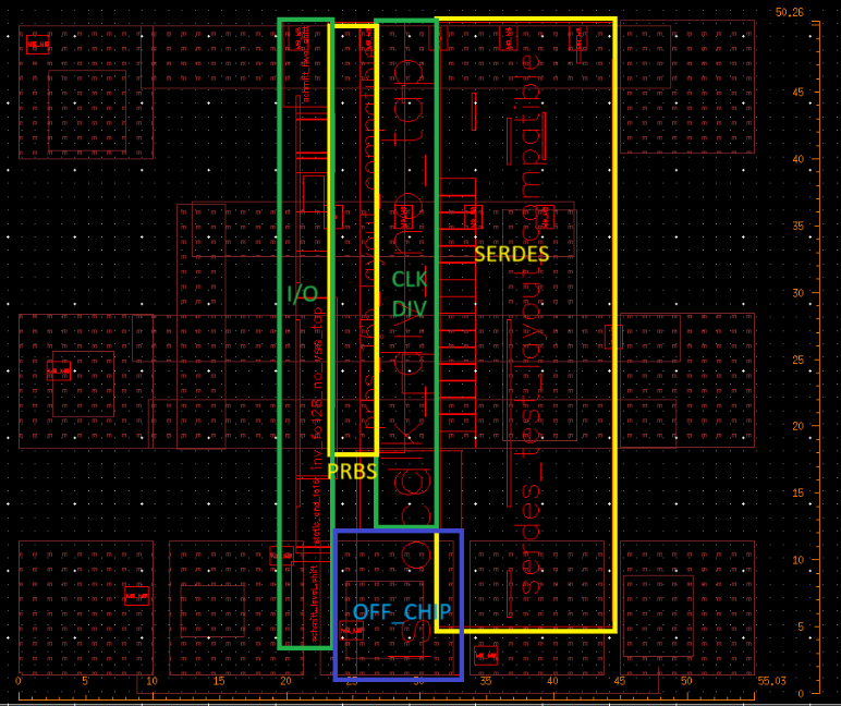 Figure 2. Layout highlighting subcomponents.
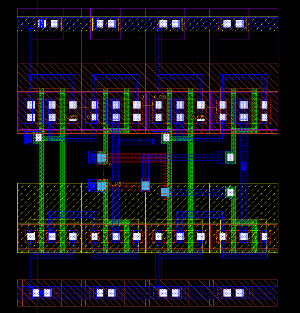 Figure 3. C2MOS Register illustrating standardization of individual layout.
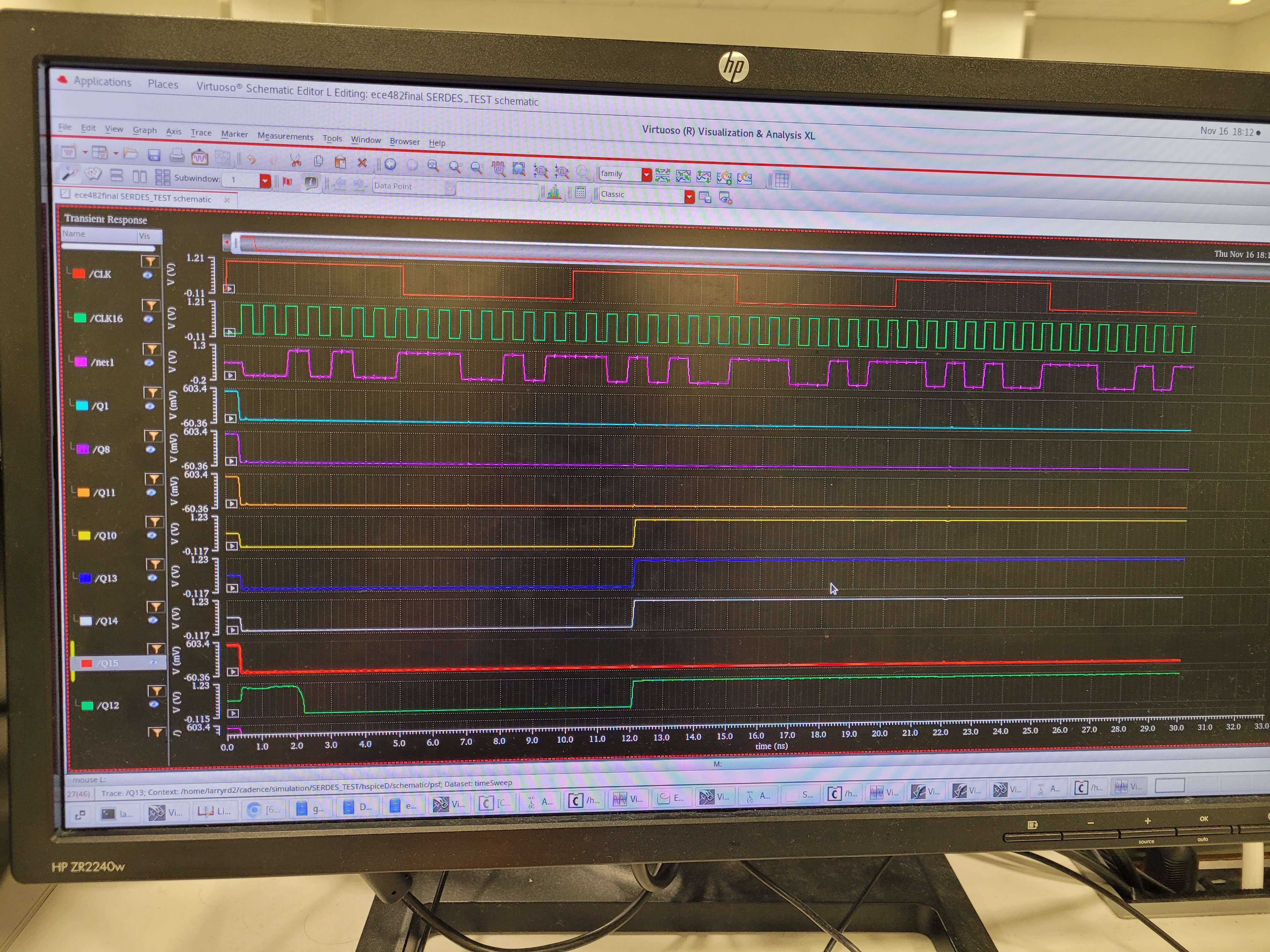 Figure 4. Waveforms illustrating PRBS and SERDES functionality.